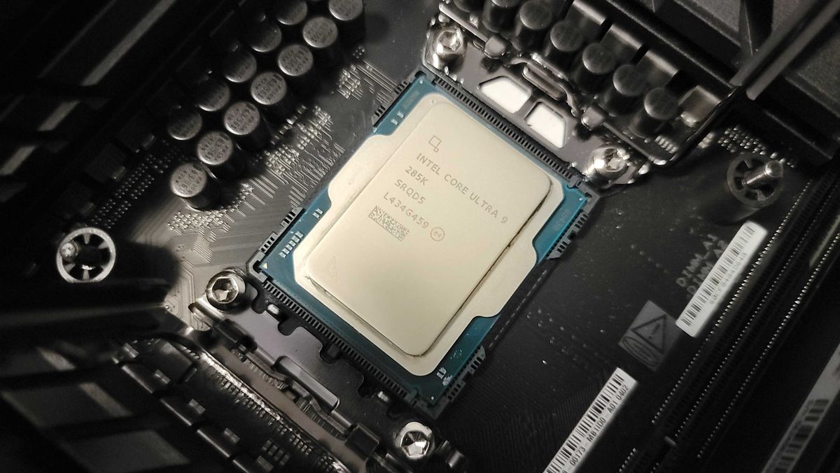
Intel’s flagship $589 Core Ultra 9 285K headlines its new ‘Arrow Lake’ Core Ultra 200S series, leading the charge with 24 cores melded into a completely new chiplet architecture that comes with plenty of new leading-edge tech, like 3D Foveros packaging, support for new DDR5 CUDIMM memory tech, and the first dedicated AI engine fused inside a desktop PC chip. However, our tests found that Arrow Lake struggles to keep pace in gaming with Intel’s own previous-gen Raptor Lake Refresh processors, never mind AMD’s chart-topping Zen 4 X3D chips.
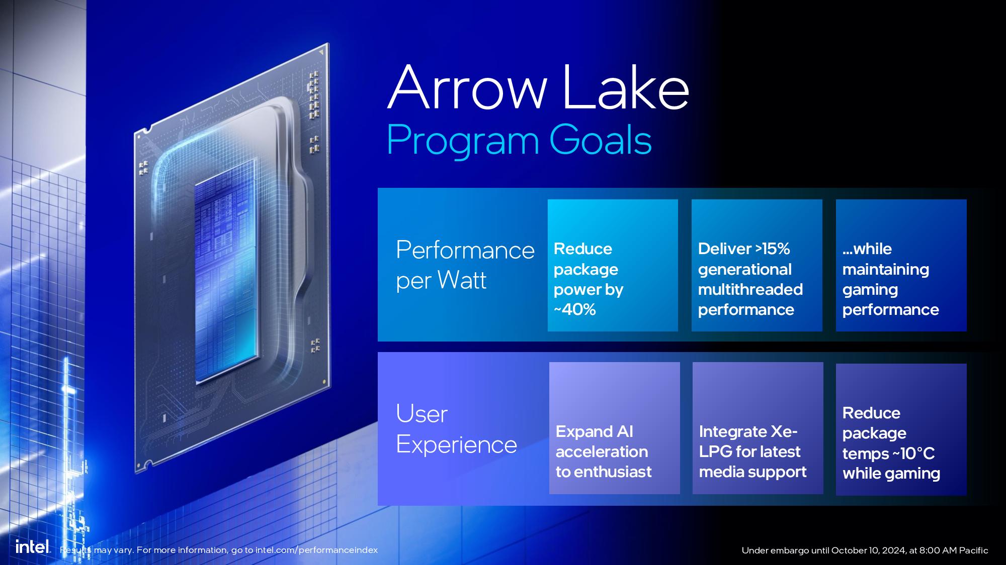
Intel says Arrow Lake provides an up to 150W reduction in system power during gaming and other improvements, like a claimed 20% gain in threaded horsepower and a 5% gain in single-thread performance over the prior-gen, which helps offset the lack of gen-on-gen gaming gains. We put those claims to the test across 14 games on the following page, not to mention a slew of productivity benchmarks.
The Intel launch comes on the heels of AMD’s tepid Zen 5 Ryzen 9000 launch, which saw AMD’s newest chips providing limited generational gaming improvements, so they couldn’t quite catch up to Intel. Naturally, given the performance we’ve seen with Intel’s new chips, AMD’s Zen 5 processors, which recently had pricing adjustments and firmware/OS enhancements, look much more promising than before — at least compared to Intel’s new chips. However, AMD also has its Ryzen 9000X3D processors slated for release early next month, and they will almost certainly be the new gaming performance champions.
That’s not to say that the Core Ultra 200S series doesn’t have its own charms. Intel employs a range of TSMC nodes for the different chiplets (called “tiles” in Intel parlance) in Arrow Lake. In fact, this marks Intel’s first mainstream desktop PC chip entirely fabricated using another company’s process node technology. Intel combines the more efficient process nodes with a radical new CPU core design that intersperses E-core clusters among the P-cores and discards Hyper-Threading entirely, thus claiming to deliver drastic power reductions that will result in a cooler and quieter PC.
| CPU | Street (MSRP) | Arch | Cores / Threads (P+E) | P-Core Base / Boost Clock (GHz) | E-Core Base / Boost Clock (GHz) | Cache (L2/L3) | TDP / PBP or MTP | Memory |
|---|---|---|---|---|---|---|---|---|
| Core Ultra 9 285K | $589 | Arrow Lake | 24 / 24 (8+16) | 3.7 / 5.7 | 3.2 / 4.6 | 76MB (40+36) | 125W / 250W | DDR5-6400 |
| Core Ultra 7 265K / KF | $394 / $379 | Arrow Lake | 20 / 20 (8+12 | 3.9 / 5.5 | 3.3 / 4.6 | 66MB (36+30) | 125W / 250W | DDR5-6400 |
| Core Ultra 5 245K / KF | $309 / $294 | Arrow Lake | 14 / 14 (6+8) | 4.2 / 5.2 | 3.6 / 4.6 | 50MB (26+24) | 125W / 250W | DDR5-6400 |
Intel’s new family spans from the $294 14-core Core Ultra 5 245KF, which we also have in our tests today, to the flagship $589 24-core Core Ultra 9 285K. Intel has the mid-range $394 20-core Core Ultra 7 265K as well, which we’ll review in the coming days.
The new Arrow Lake chips require an 890-series motherboard, and vendors have a wide range of Z890 models available. You can also now opt for either standard DDR5 or the new CUDIMM DDR5 modules, which boost easily attainable memory overclocking speeds to DDR5-8000 and beyond. However, Intel no longer supports both DDR4 and DDR5 memory like it did with the prior-gen Raptor Lake processors.
Intel Core Ultra 9 285K Pricing and Specifications
Intel’s generational branding stopped at the 14th-Gen family — there will be no 15th-Gen. Instead, Intel has now switched to the same ‘Core Ultra’ branding it uses for the mobile market and uses the ‘S’ suffix to differentiate the desktop models. Intel begins the new ‘Core Ultra’ desktop series at ‘200S’ instead of ‘100S.’ So, no, you didn’t miss a generation anywhere; Intel just can’t seem to make a coherent branding decision.
The five Arrow Lake SKUs slot into the Ultra 9, 7, and 5 families, spanning chips with 24, 20, and 14 cores, matching their prior-gen counterparts. However, the Performance cores (P-cores) no longer support Hyper-Threading, so total thread counts are now lower. Intel says it has increased overall performance in multi-threaded workloads despite removing Hyper-Threading, which largely holds up in our testing.
Intel has standard overclockable K-series models and two KF-series Core 7 and 5 chips that come without the integrated graphics engine. Intel doesn’t have a KF option for the Ultra 9 285K, and it remains to be seen if one will come to the market in the future.
| CPU | Street (MSRP) | Arch | Cores / Threads (P+E) | P-Core Base / Boost Clock (GHz) | E-Core Base / Boost Clock (GHz) | Cache (L2/L3) | TDP / PBP or MTP | Memory |
|---|---|---|---|---|---|---|---|---|
| Ryzen 9 7950X3D | $599 ($699) | Zen 4 X3D | 16 / 32 | 4.2 / 5.7 | — | 144MB (16+128) | 120W / 162W | DDR5-5200 |
| Ryzen 9 9950X | $599 ($599) | Zen 5 | 16 / 32 | 4.3 / 5.7 | — | 80MB (16+64) | 170W / 230W | DDR5-5600 |
| Core Ultra 9 285K | $589 | Arrow Lake | 24 / 24 (8+16) | 3.7 / 5.7 | 3.2 / 4.6 | 76MB (40+36) | 125W / 250W | CUDIMM DDR5-6400 / DDR5-5600 |
| Core i9-14900K / KF | $445 K / $442 KF | Raptor Lake Refresh | 24 / 32 (8+16) | 3.2 / 6.0 | 68MB (32+36) | 125W / 253W | DDR4-3200 / DDR5-5600 | |
| Ryzen 9 7900X3D | $579 ($599) | Zen 4 X3D | 12 / 24 | 4.4 / 5.6 | — | 140MB (12+128) | 120W / 162W | DDR5-5200 |
| Ryzen 7 7800X3D | $476 ($449) | Zen 4 X3D | 8 / 16 | 4.2 / 5.0 | — | 104MB (8+96) | 120W / 162W | DDR5-5200 |
| Ryzen 9 9900X | $429 ($469) | Zen 5 | 12 / 24 | 4.4 / 5.6 | — | 76MB (12+64) | 120W / 162W | DDR5-5600 |
| Core Ultra 7 265K / KF | $394 / $379 | Arrow Lake | 20 / 20 (8+12 | 3.9 / 5.5 | 3.3 / 4.6 | 66MB (36+30) | 125W / 250W | CUDIMM DDR5-6400 / DDR5-5600 |
| Core i7-14700K / KF | $354 K / $327 KF | Raptor Lake Refresh | 20 / 28 (8+12) | 3.4 / 5.6 | 2.5 / 4.3 | 61MB (28+33) | 125W / 253W | DDR4-3200 / DDR5-5600 |
| Core i5-14600K / KF | $256 K / $229 KF | Raptor Lake Refresh | 14 / 20 (6+8) | 3.5 / 5.3 | 2.6 / 4.0 | 44MB (20+24) | 125W / 181W | DDR4-3200 / DDR5-5600 |
| Ryzen 7 9700X | $326 ($329) | Zen 5 | 8 / 16 | 3.8 / 5.5 | — | 40MB (8+32) | 65W / 88W | DDR5-5600 |
| Core Ultra 5 245K / KF | $309 / $294 | Arrow Lake | 14 / 14 (6+8) | 4.2 / 5.2 | 3.6 / 4.6 | 50MB (26+24) | 125W / 250W | CUDIMM DDR5-6400 / DDR5-5600 |
| Ryzen 5 9600X | $249 ($249) | Zen 5 | 6 / 12 | 3.9 / 5.4 | — | 38MB (6+32) | 65W / 88W | DDR5-5600 |
Intel’s Ultra 9 weighs in at $589, matching the launch pricing of the previous-gen equivalent, the Core i9-14900K. The $394 Ultra 7 265K debuts for $15 less than the previous-gen Core i7-14700K it replaces, while the $309 Core 5 245K is $10 less than the prior-gen Core i5-14600K.
Intel made numerous adjustments to the stack, including reductions in peak clock speeds — a somewhat expected byproduct of moving to TSMC’s N3B process node. The Ultra 9 peaks at 5.7 GHz, 300 MHz less than the prior-gen 14900K’s blistering 6 GHz boost, while the Ultra 7 and 5 boost clocks see 100 MHz reductions. However, Intel has adjusted P-core base clocks upward by 500 to 700 MHz. The E-cores also have boose clock improvements spanning from 200 to 600 MHz, and a 600 MHz to 1 GHz improvement in base clock speeds, all of which vary by model.
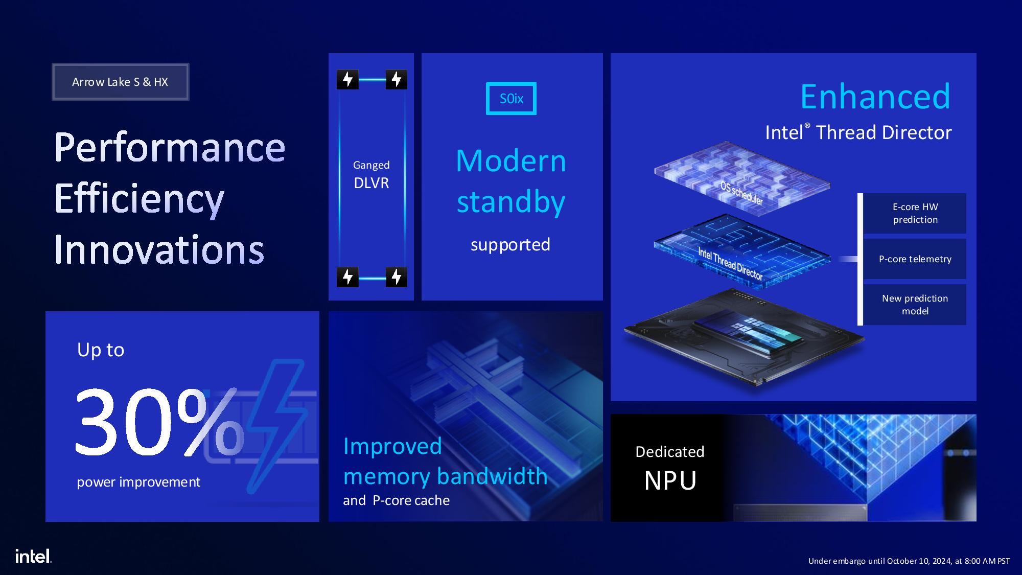
Despite Arrow Lake’s claimed lower operating power consumption, the chips still have similar maximum TDP (MTP) ratings of 250W for Ultra 9 and 7 (3W less than Raptor Lake) and 159W (22W less) for the Ultra 5 model. Intel says the lower power consumption occurs during normal workloads with an up to 40% reduction in package power consumption. Intel also increased the maximum CPU temperature (TJMax) to 105C for Arrow Lake, which is 5C higher than its traditional limit with mainstream PC processors.
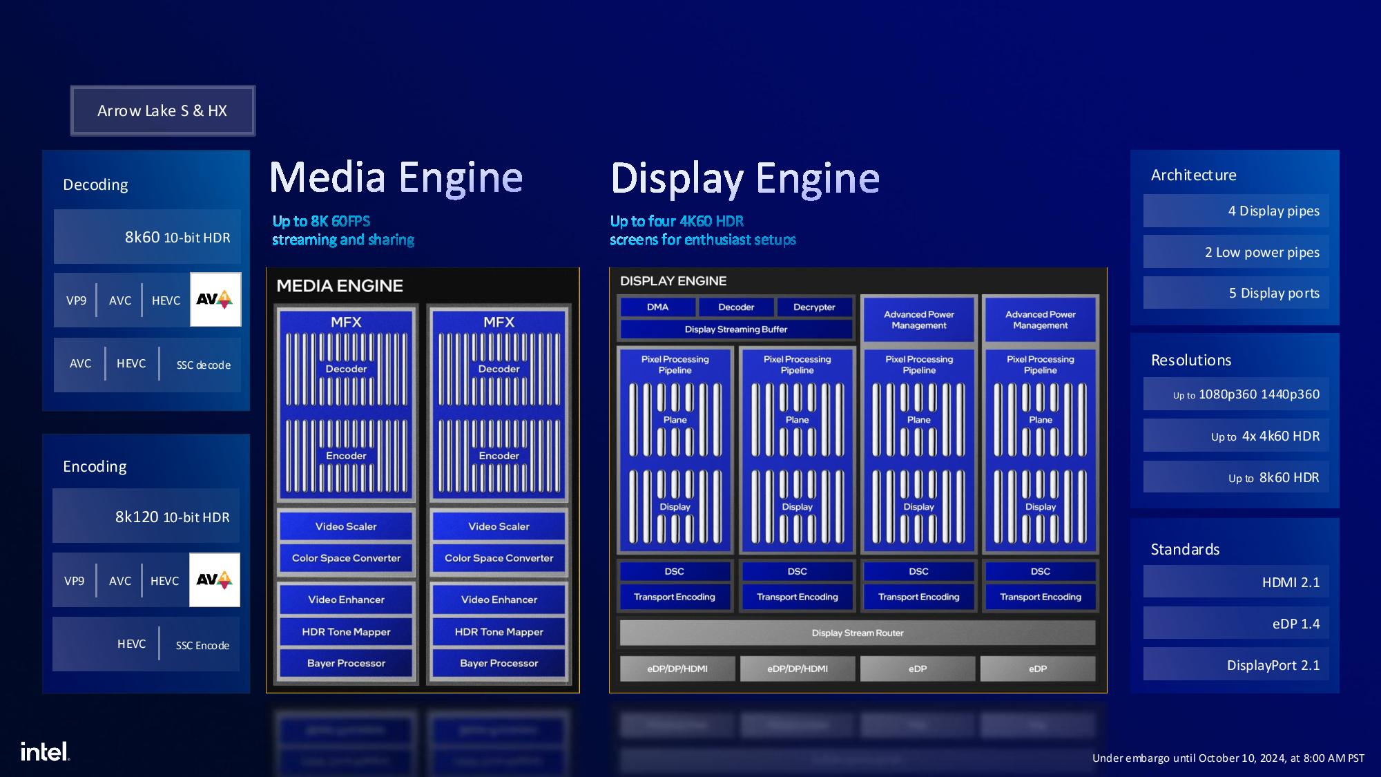
The new chips come with 24 lanes of PCIe 5.0 support, with an additional 20 PCIe 4.0 lanes provided by the chipset. The Ultra 9, 7, and 5 all have the same Xe-LPG graphics engine with four Xe cores — the same GPU as the Meteor Lake chips, not the newer Battlemage Xe2 engine found in the Lunar Lake mobile chips. The Ultra 9 and 7 iGPU have a 2.0 GHz graphics boost clock, while the Ultra 5 drops to 1.9 GHz. Intel claims the iGPU offers twice the performance of the graphics on the 14th-gen processors, but we haven’t yet had time to put those claims to the test. Also, integrated graphics performance on a desktop chip largely won’t matter for many users, as if you actually care about GPU performance you just add a discrete graphics card.
The chips also feature the same in-built NPU engine for AI acceleration as Meteor Lake — not Lunar Lake. This engine provides up to 13 TOPS of INT8 throughput, but that doesn’t meet Microsoft’s requirement of 40+ TOPS to unlock Copilot+ features. Intel already has a larger NPU design in the market — the (up to) 48 TOPS engine found in Lunar Lake — but used the smaller engine to optimize the die area for the desktop PC market. A larger engine would chew into the space available for other additives, like cores and cache. Intel says it hasn’t seen enough interest in the desktop PC market yet to sacrifice other areas of performance for the NPU. As with the iGPU, the decision makes sense: If you care about AI compute, even Nvidia’s lowest tier RTX 4060 offers 242 TOPS of INT8 performance.
Arrow Lake drops into the LGA 1851 socket, so the chips are incompatible with existing motherboards. Existing coolers should be compatible with the requisite mounting hardware, but the need for a kit could vary by vendor. Intel hasn’t committed to using the LGA 1851 socket for future processor generations. We’ve seen signs of a Core Ultra 2000S Refresh generation in the works, but that isn’t yet confirmed. That could mean that LGA 1851 will end up as a single-generation socket.
CUDIMMs and Memory Support Matrix
Arrow Lake supports up to 192GB of DDR5 memory, but now in two flavors with two different base speeds. The chips support DDR5-6400 with DDR5 CUDIMMs, a new type of DIMM with an integrated clock driver (ckd) that boosts easily attainable stable clock frequencies by amplifying the signal, thus stabilizing the data eye. Unlike the clock redrivers present on fully-buffered registered DIMMs, the CUDIMM redrivers are said not to impose an additional clock cycle of latency (they use a less complicated and cheaper design).
Intel also points to much higher overclocking headroom with CUDIMMs and says DDR5-8000 appears to be the sweet spot (Gear 2). CUDIMMs should enable the use of poorer-quality DRAM ICs in higher-speed kits while simplifying the pricier DIMM PCB designs often required for higher-end memory. But motherboards with CUDIMM support may cost extra, and the CUDIMMs themselves are likely to carry a price premium, so you’ll need to pay close attention to the final cost before deciding whether CUDIMMs make sense.
Intel also supports standard DDR5, but at lower base speeds than it supports with CUDIMMs (the same DDR5-5600 as with its 14th Gen CPUs). Naturally, both types of memory are overclockable. The Arrow Lake DDR5 support matrix is in the table below. Arrow Lake does support ECC memory, but it won’t be supported on consumer platforms — instead, that feature is reserved for enterprise-focused W-series motherboards.
| DRAM Config | Official Speeds Supported |
| Dual Channel, 2 board slots, 2 UDIMMs | DDR5-5600 |
| Dual Channel, 2 board slots, 2 CUDIMMs | DDR5-6400 |
| Dual Channel, 4 board slots, 2 UDIMMs | DDR5-5600 |
| Dual Channel, 4 board slots, 2 CUDIMMs | DDR5-5600 |
| Dual Channel, 4 board slots, 4 UDIMMs | DDR5-4800 (single rank DIMMs) DDR5-4400 (dual rank DIMMs) |
| Dual Channel, 4 board slots, 4 CUDIMMS | DDR5-4800 (single rank DIMMs) DDR5-4400 (dual rank DIMMs) |
Intel Arrow Lake Core Ultra 200S architecture
Arrow Lake marks Intel’s first foray into a disaggregated architecture, meaning that different compute and I/O functionalities are split out into their own dies. Intel refers to its die disaggregation technique as a ‘tiled’ architecture, but the rest of the industry refers to this as a chiplet architecture. Intel says that a ‘tiled’ processor refers to a chip using advanced packaging, which enables parallel communication between the chip units, while standard packaging employs a serial interface that isn’t as performant or energy efficient. However, other competing processors with advanced packaging are still referred to as chiplet-based, so the terms are largely interchangeable.
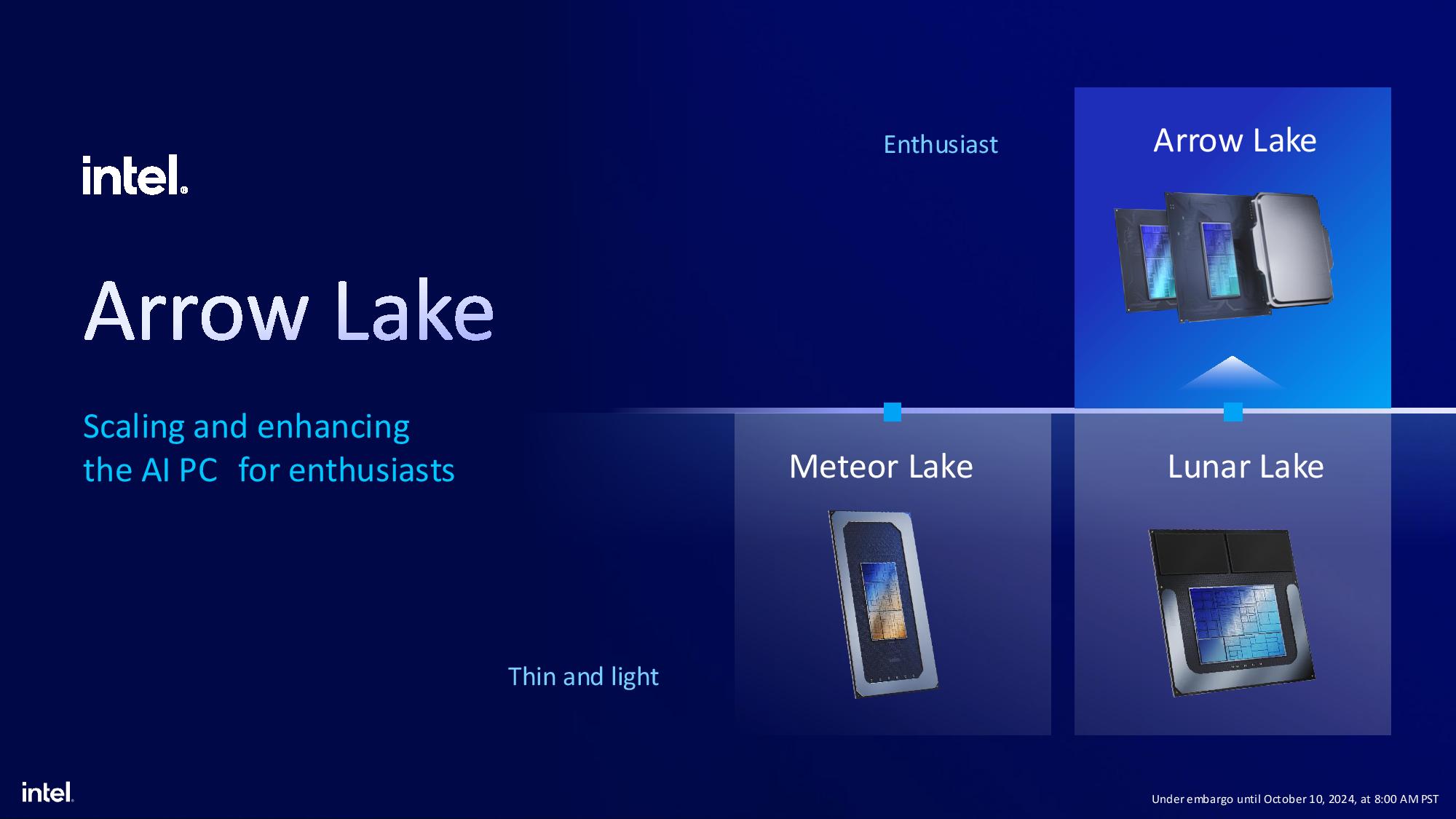
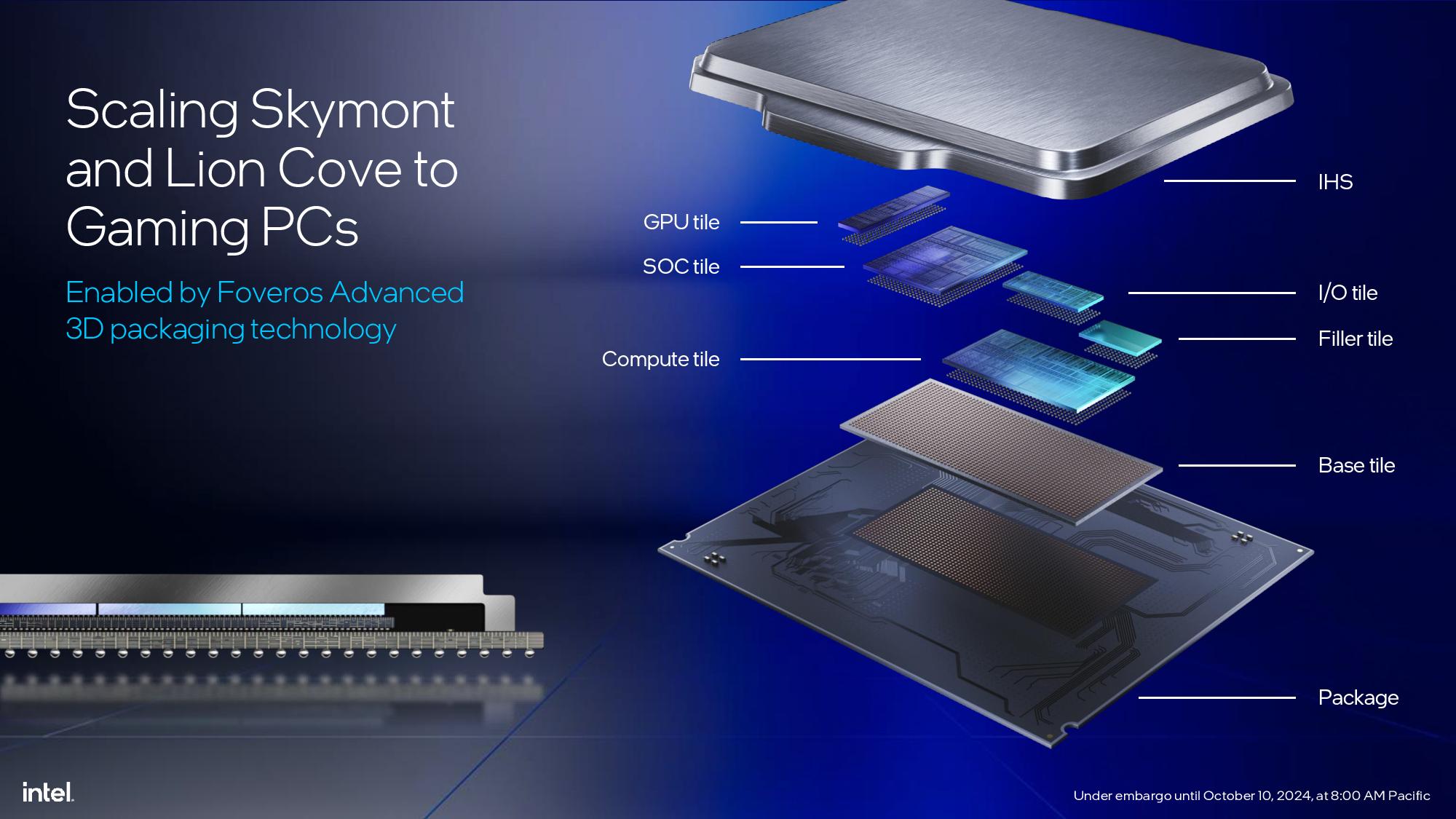
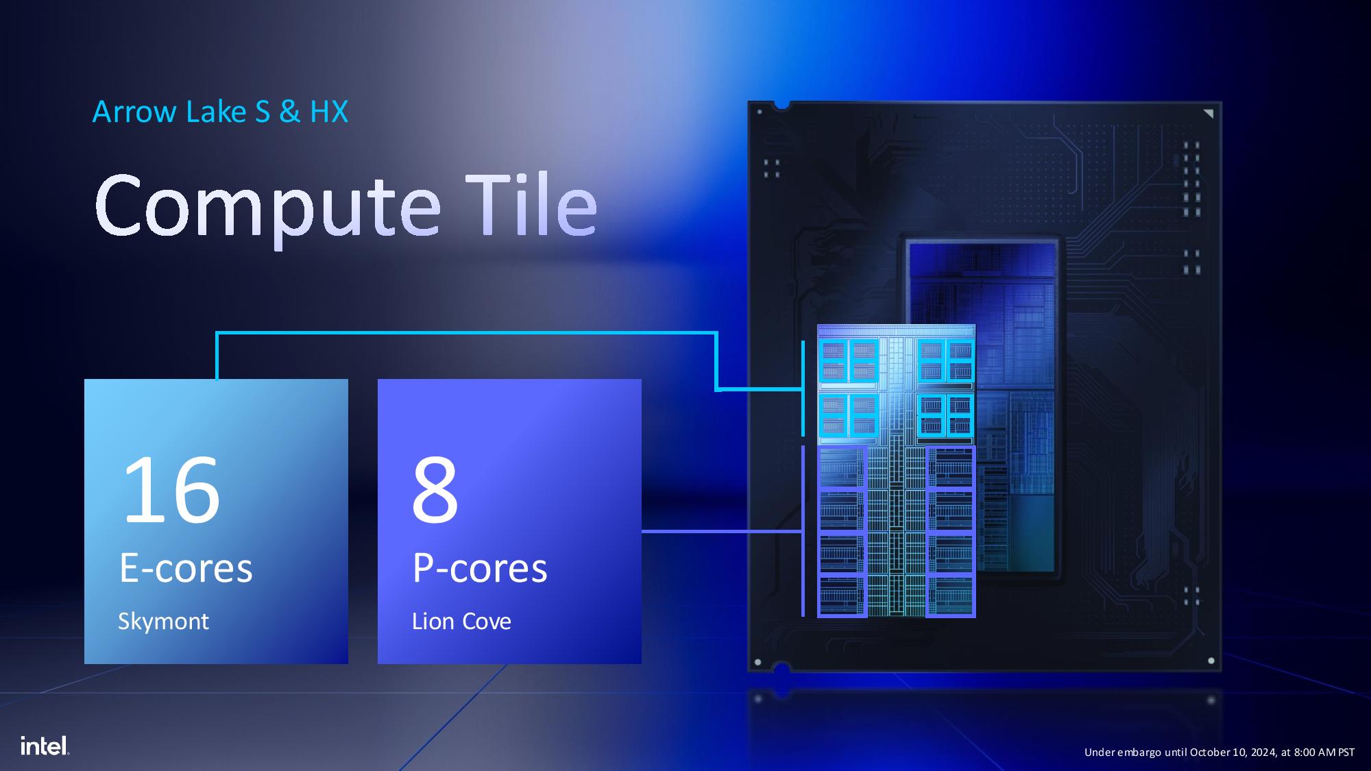
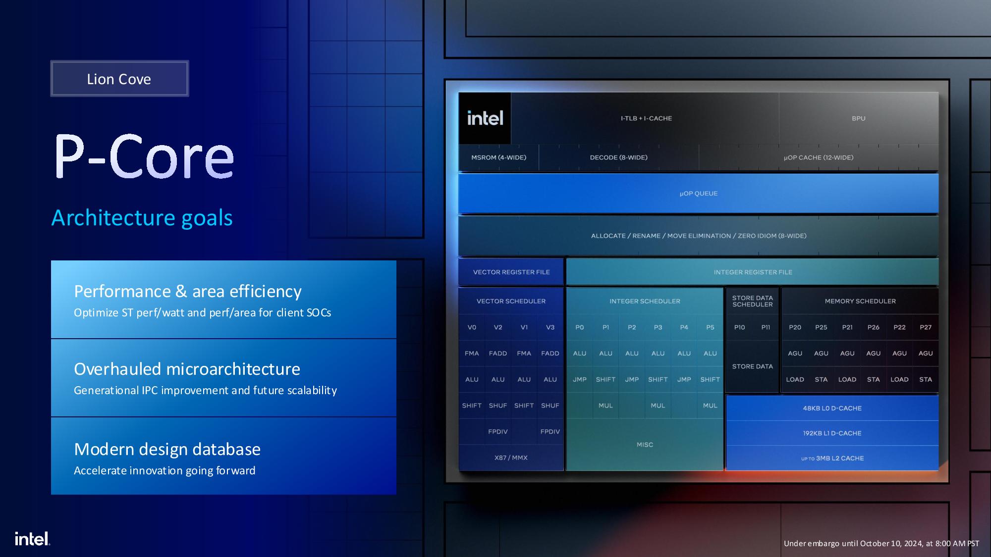
Instead of the newer Lunar Lake design, Arrow Lake uses a package design similar to its five-tile previous-gen Meteor Lake laptop processors. However, Intel integrated the newer Lion Cove P-core and Skymont E-core microarchitectures for the compute tile instead of the Redwood Cove and Crestmont cores it used in Meteor Lake.
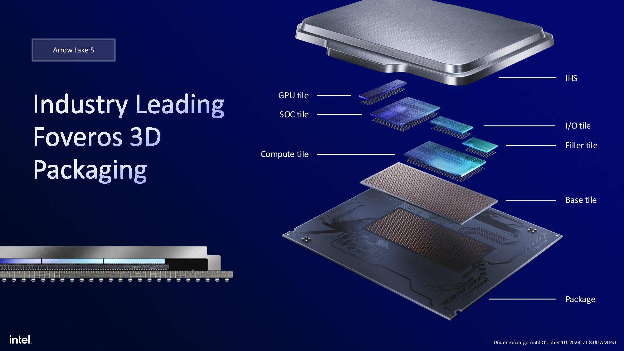
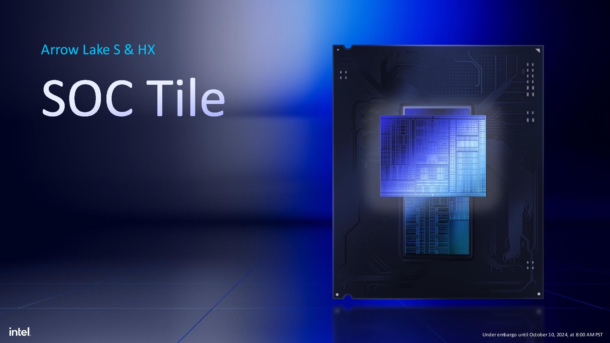
The Arrow Lake design employs Intel chip designs etched on a compute tile (chiplet) fabbed on the TSMC N3B process node, a GPU tile with the TSMC N5P node, while the SoC and I/O tiles use TSMC’s N6 process. Intel uses Foveros 3D packaging to mount those tiles to an underlying base tile fabbed on the Intel 1227.1 process node (22nm FinFET). There are also two ‘dummy’ filler tiles that provide mechanical rigidity.
| Row 0 – Cell 0 | Arrow Lake – Manufacturer / Node | Meteor Lake – Manufacturer / Node |
| CPU Tile | TSMC / N3B (3nm) | Intel / ‘Intel 4’ |
| 3D Foveros Base Die | Intel / 22FFL (Intel 16) | Intel / 22FFL (Intel 16) |
| GPU Tile (tGPU) | TSMC / N5P (5nm) | TSMC / N5 (5nm) |
| SoC Tile | TSMC / N6 (6nm) | TSMC / N6 (6nm) |
| IOE Tile | TSMC / N6 (6nm) | TSMC / N6 (6nm) |
Intel says the chip has 17.8 billion transistors spread out over a total die area of 243mm^2. Unfortunately, given the different nodes employed and the fact that Intel included the filler tiles in the total die area, that doesn’t tell us much about transistor density.
Intel’s decision to split the memory controller and PHY into their own tile (I/O tile) was to improve yields, but this creates memory latency issues that contribute to the lower gaming performance we see on the next page. Intel does offer the option to overclock the tile-to-tile interface, but we haven’t had a chance to test the impact yet. Here’s the memory latency we measured with AIDA, and our cache and memory latency benchmarks using the Memory Latency tool from the Chips and Cheese team soon.
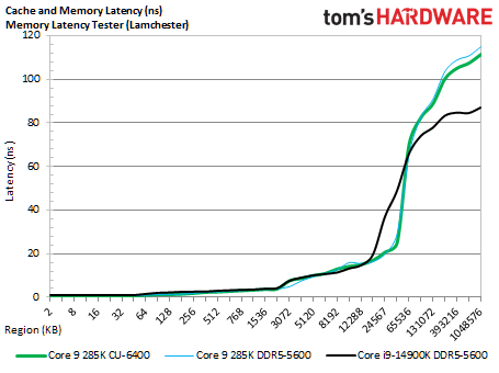
| Memory Latency – Tom’s Hardware | DDR5-5600 | CUDIMM DDR5-6400 | L3 Latency |
| Core Ultra 9 285K | 94.1 ns | 91.9 ns | 16.6 / 15.8 ns |
| Core i9-14900K | 79.1 ns | N/A | 21.8 ns |
As you can see in the AIDA tests, on a like-for-like basis with DDR5-5600, the remote memory controller and PHY add 15 ns of memory latency in our test. Intel says we can expect a 15 to 20 ns increase in memory latency for Arrow Lake. That’s a pretty significant change, and not in a good way. It will definitely impact certain workloads, gaming in particular.
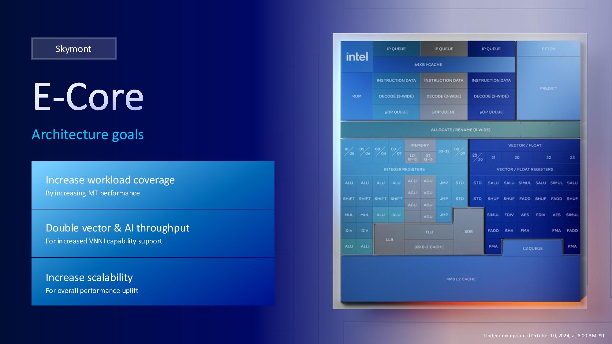
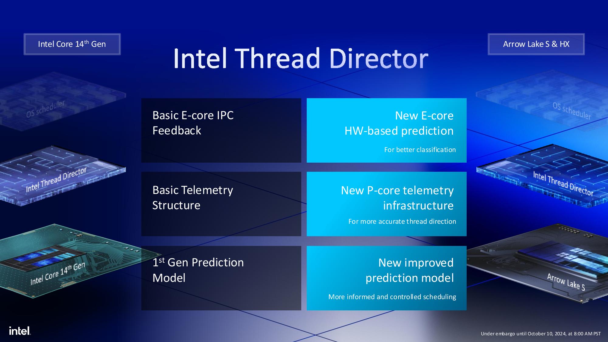
Intel redesigned its CPU core layout for Arrow Lake, with quad-core E-core clusters interspersed among the P-cores. Previously, Intel placed all the E-cores in their own dedicated block. Intel spread the cores out to reduce hotspots for this design.
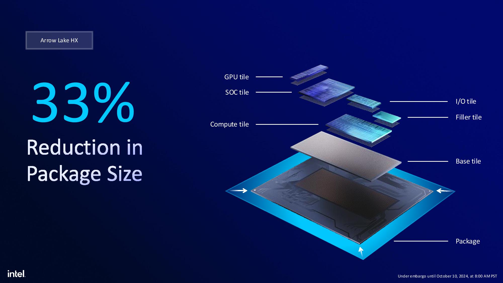
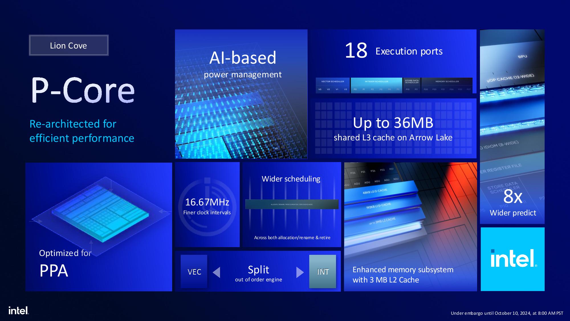
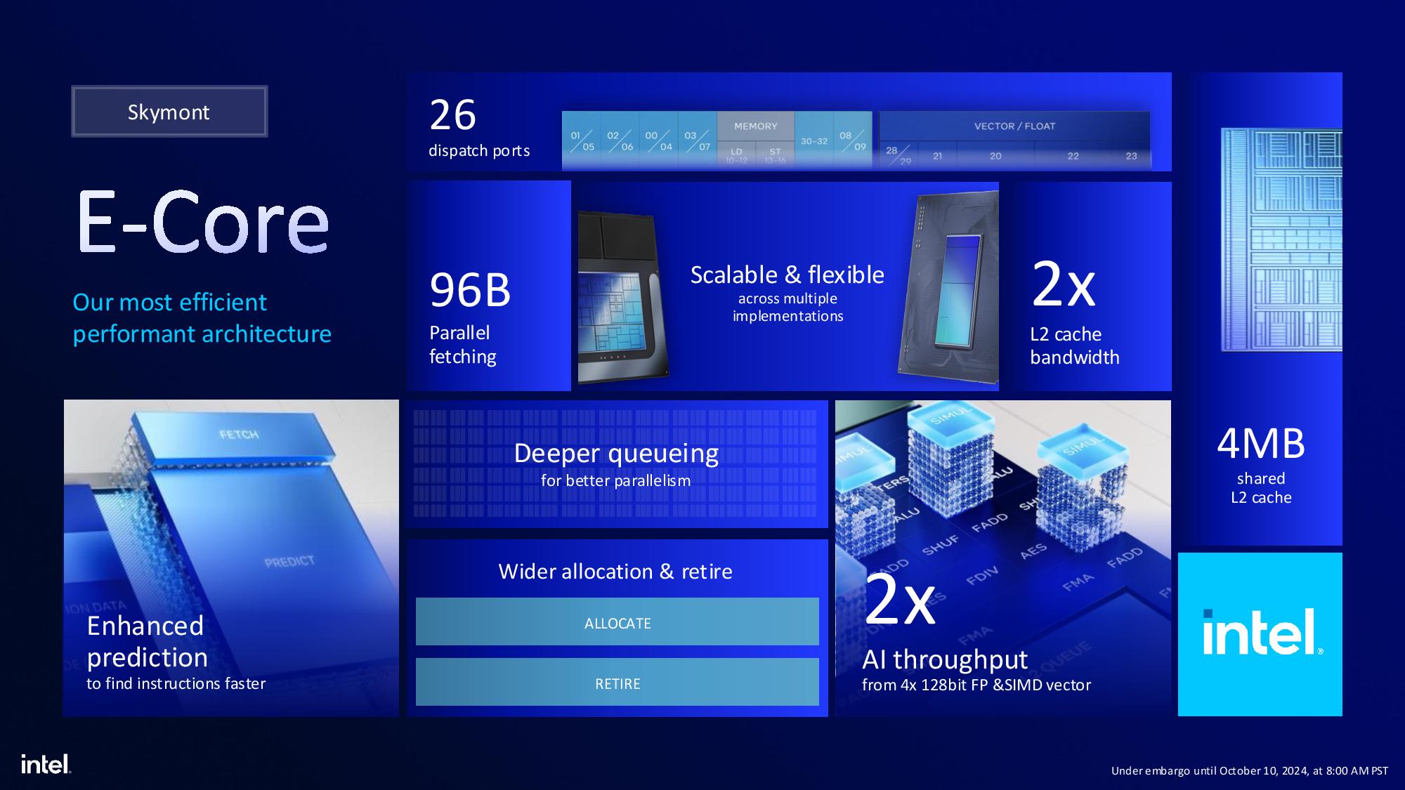
Intel also connected the E-cores to the 36MB L3 cache, so they now share L3 with the P-cores for the first time. The P-cores and E-cores still have dedicated L2 caches, with 3MB for the P-cores (a .5MB increase over the prior gen) and 4MB of L2 shared among each E-core cluster. Intel says the new design yielded a 33% reduction in package size and allowed it to quickly port innovations from Lunar Lake to Arrow, thus allowing it to launch the two chips a mere month apart.
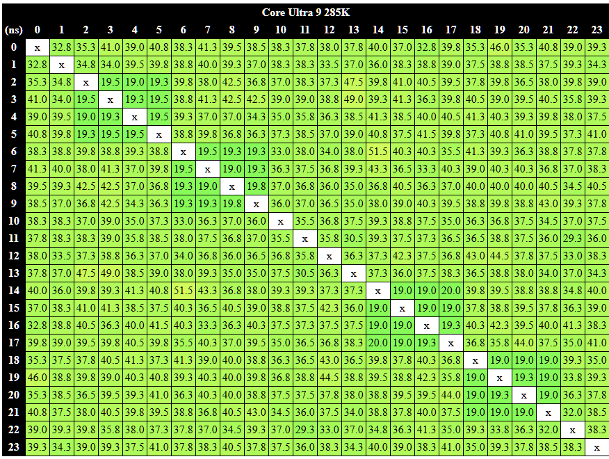
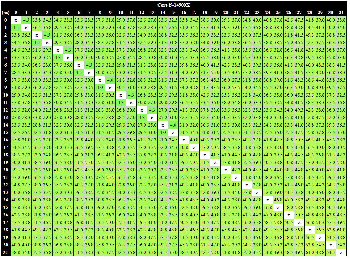
The album below contains a latency heatmap for both the new design and the previous-gen Core 9-14900K, showing that the removal of Hyper-Threading has greatly simplified the core-to-core traffic due to the reduced number of threads.
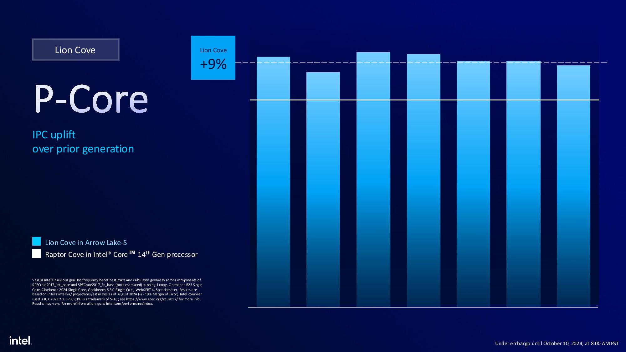
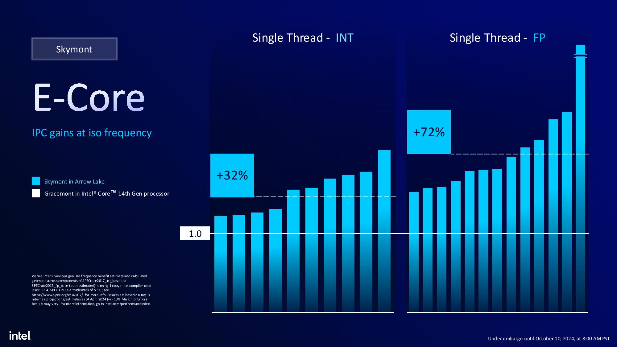
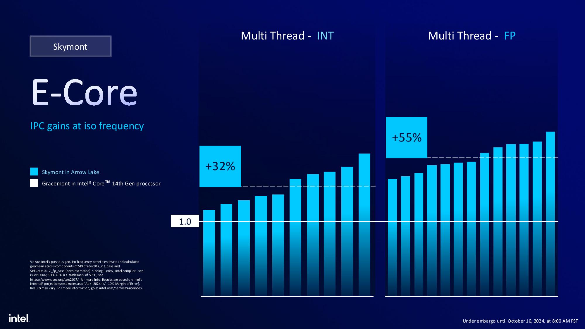
We’ve also included the slides detailing the advances of the P-core and E-core architectures, but we’ve already covered these microarchitectures in-depth in our Lunar Lake deep dive. Overall, Intel claims a 9% increase in IPC over Raptor Lake (lower than the 14% cited with Lunar Lake because Intel made that comparison to Meteor Lake), a 32% increase in integer IPC, and a 72% increase in floating point IPC for the E-cores.
But claims and architectural details are only the foundation. Let’s see how everything looks like in actual real-world performance testing and benchmarks on the following pages.

